How to select photoplotter for pcb making ?

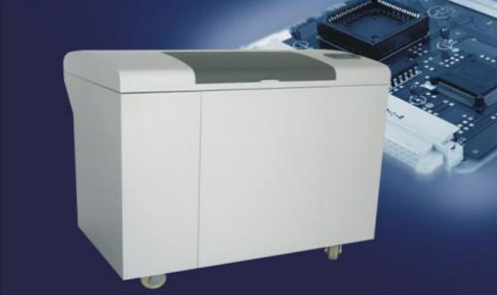
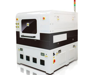
The hardware indexes of laser photoplotter are mainly reflected in the following aspects: positioning accuracy, format, resolution, uniformity, optical system quality and reliability.
The development of the downstream PCB industry promotes the growth of PCB ink demand: In recent years, the manufacturing industry led by the electronic information industry has shifted to the Asia-Pacific region. The global PCB manufacturing center has grown rapidly in the Asia-Pacific region. China's PCB output value has increased significantly, and China's PCB industry status has continued to strengthen. According to data from the China Business Industry Research Institute, China's PCB output value has reached 32.9 billion yuan in 2019, and will further rise to 35.1 billion yuan in 2020.
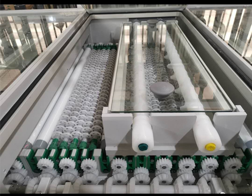
The choice of etching solution is very important because it directly affects the accuracy and quality of high-density thin wire image in the manufacturing process of printed circuit board. Of course, the etching characteristics of etching solution are affected by many factors, including physical, chemical and mechanical aspects.
Fiber laser cutting machines have replaced most markets such as CO2 high-power laser cutting machines, YAG laser cutting machines and disc laser cutting machines. Fiber laser cutting machine is developing towards more refinement, industrialization, deep customization and supporting.
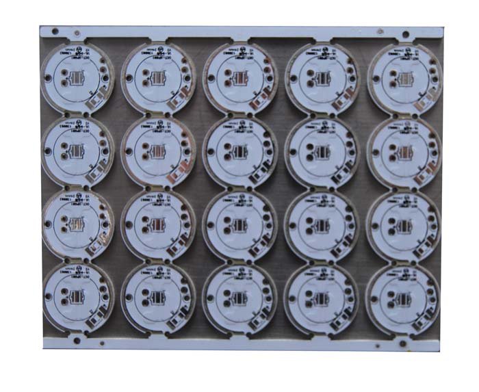
There are two making process, the pattern exposure process and the pattern silk screen process. The pattern exposure process price is higher than the pattern silk screen process, the utility is just to make the circuit better looking? The circuit of the pattern silk screen process can still operate. The exposure process has a higher price, but less utility. So what is the difference between the pattern exposure process and the pattern silk screen process of aluminum substrate?
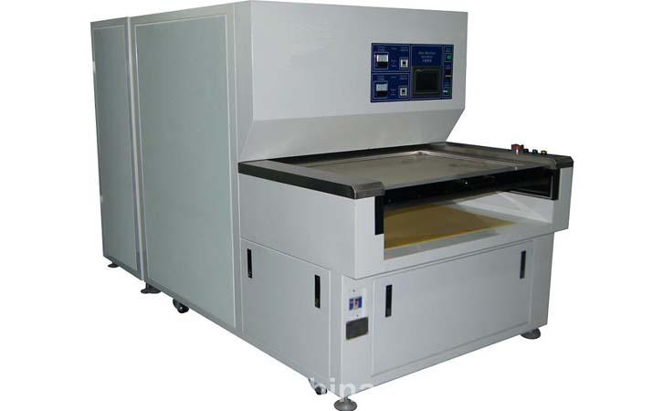
UV exposure machine is an essential equipment for modern PCB manufacturing. In the PCB manufacturing process, one of the most key processes is to transfer the negative image to the copper foil substrate. First, a layer of photosensitive material (such as liquid photosensitive adhesive, photosensitive resist dry film, etc.) is coated on the substrate, and then the photosensitive material coated on the substrate is irradiated to change its solubility. The resin of the non photosensitive part is not polymerized and dissolved under the action of the developer, and the resin of the photosensitive part remains on the substrate to form an image. This process is exposure, That is, the process completed by the exposure machine in the production of printed circuit board.