PCB hole copper plated cavity Occurrence and Countermeasures
Jan. 04, 2023PTH is a very important step in the hole metallization process of PCB circuit board. Its purpose is to form an extremely thin conductive copper layer …
PTH is a very important step in the hole metallization process of PCB circuit board. Its purpose is to form an extremely thin conductive copper layer …
How to distinguish HDI PCB Primary pressing, Twice pressing and Triple pressing HDI board (High Density Interconnector), namely high-density interconn…
Electroplated copper layer has the advantages of good conductivity, thermal conductivity and mechanical ductility, and is one of the indispensable key…
At present, printed circuit board is still the main assembly mode of electronic equipment used for various electronic equipment and systems. Practice …
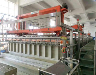
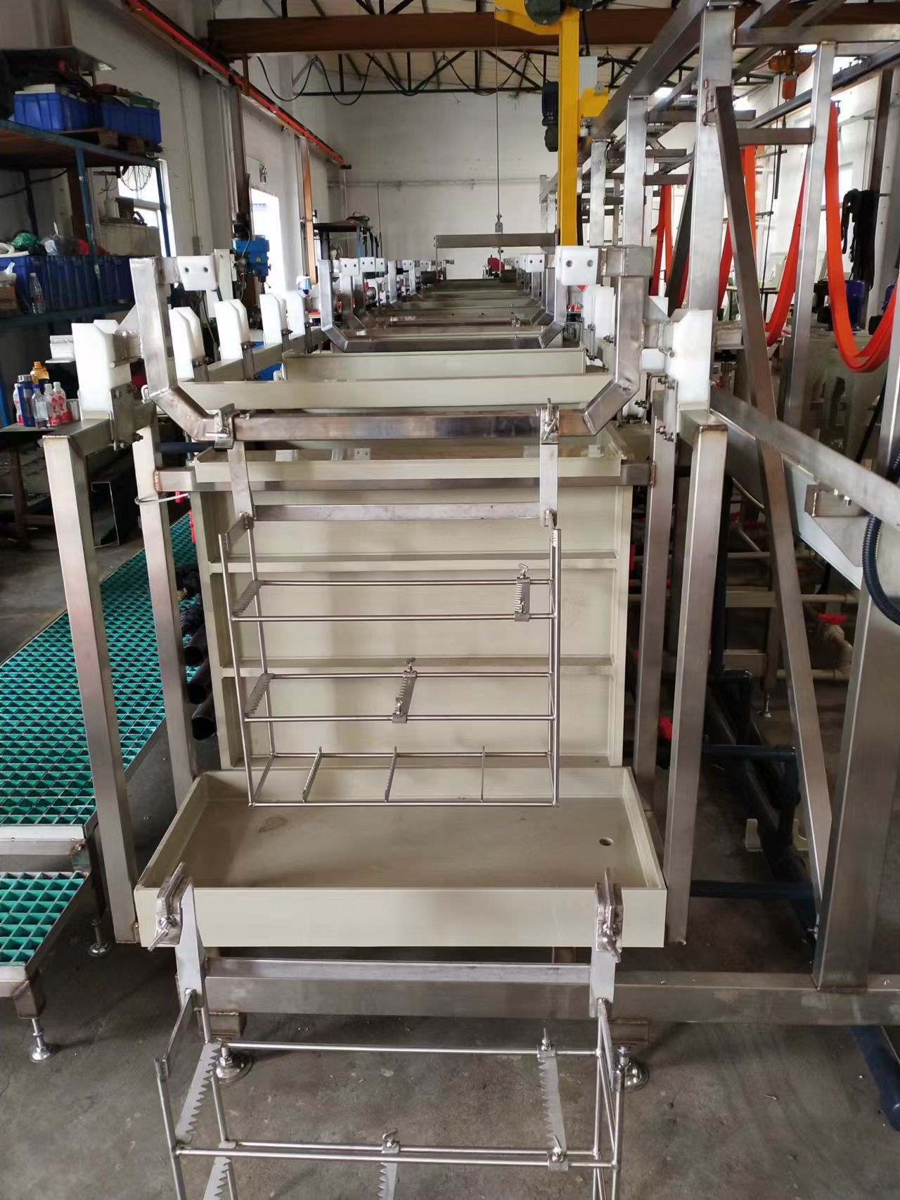
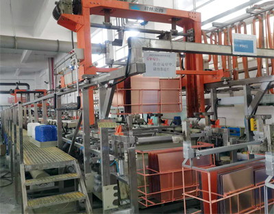
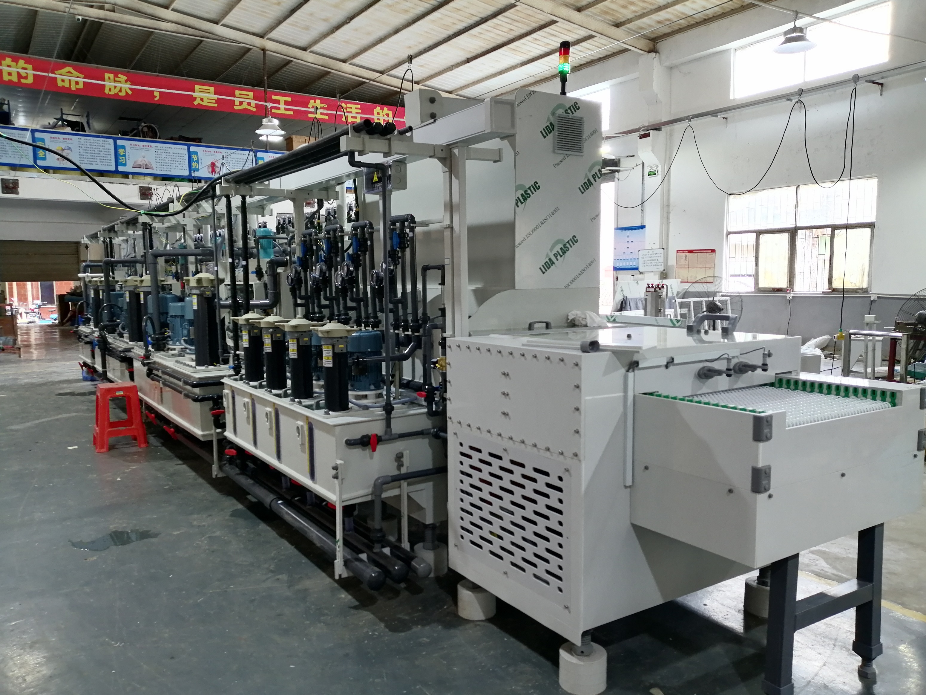
In the production process of printed circuit board, there are two kinds of main electroplating equipment, one is horizontal electroplating line, the o…
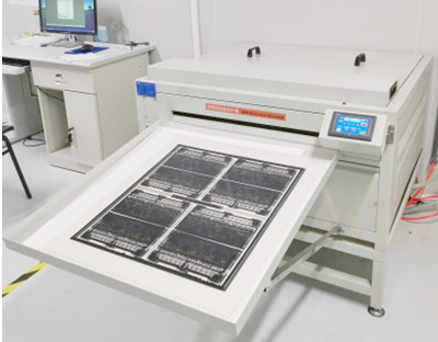
1、 Causes and solutions of negative film deformation: Reason: (1) Temperature and humidity control failure (2) The temperature rise of the exposure ma…