Work principle and process of PCB laser photoplotter
Jun. 15, 2022Laser photoplotter, referred to as photoplotter, is a phototypesetting product integrating laser optical technology, microelectronic technology and ul…
Laser photoplotter, referred to as photoplotter, is a phototypesetting product integrating laser optical technology, microelectronic technology and ul…
The process of printed circuit board from optical board to showing circuit pattern is a complex physical and chemical reaction process. This paper ana…
Most holes, including NPTH and PTH holes, will be drilled on the pressed plate during initial drilling. When drilling PTH hole, the diameter of the ho…
The surface treatment of PCB striking board includes OSP, gold precipitation, bare copper, Hard zinc plating, and the most common HASL. HASL can be di…
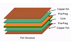
In the manufacture of PCB, the lamination process usually refers to the lamination of copper foil, prepreg and the core board (inner layer) with a pre…
Tin spraying, also known as hot air solder leveling (HASL), is to coat a layer of tin-lead alloy on the copper surface to prevent oxidation of the cop…