
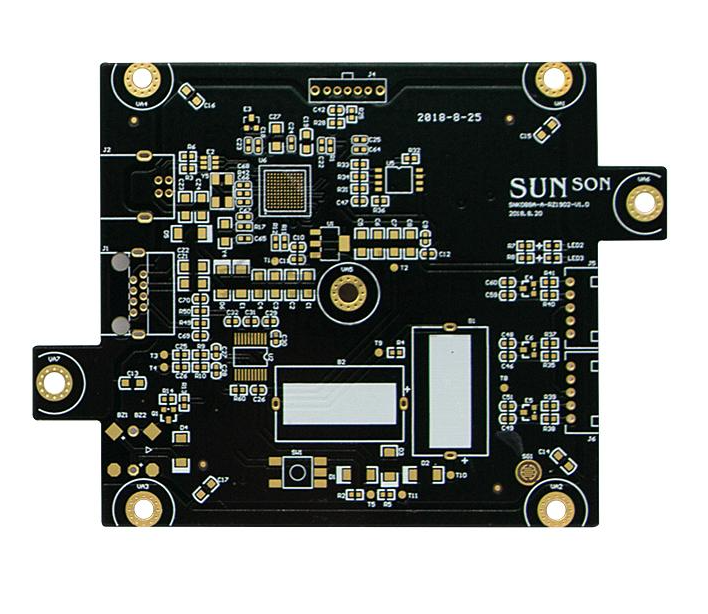
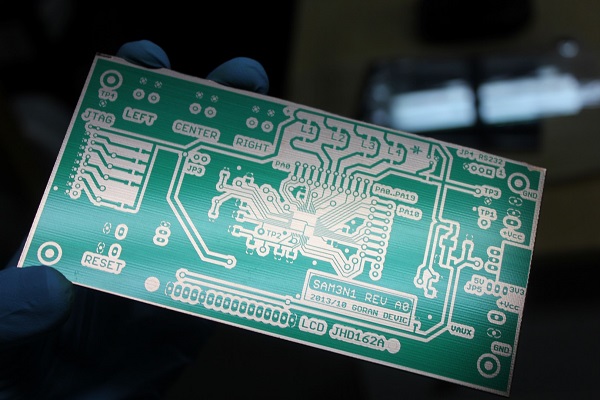
Let’s first introduce the common drilling holes in PCB: Plated through hole, blind via hole and buried via hole. The meaning and characteristics of these three holes.
Plated through hole (VA), a common hole, is used to conduct or connect copper foil circuits between conductive patterns in different layers of circuit board. For example, for example, blind hole and buried hole, but can not insert the copper plated hole of the assembly leg or other reinforcing material. Because PCB is formed by stacking and accumulating many copper foil layers, an insulating layer will be paved between each copper foil layer, so that the copper foil layers cannot communicate with each other, and the signal link depends on the through hole (IA), so it has the title of Chinese through hole.
The characteristics are: in order to meet the needs of customers, the through hole of the circuit board must be plugged. In this way, in changing the traditional aluminum plug hole process, the resistance welding and plug hole of the circuit board surface are completed with white mesh, so that the production is stable, the quality is reliable and the application is more perfect. The through hole mainly plays the role of connecting and conducting circuits. With the rapid development of the electronic industry, it also puts forward higher requirements for the manufacturing process and surface mount technology of printed circuit board. The process of plug hole for through hole is applied, and the following requirements should be met: 1. If there is copper in the through hole, it can be plugged without resistance welding. 2. There must be tin lead in the through hole, with a certain thickness requirement (4um). No solder resist ink shall enter the hole, resulting in hidden tin beads in the hole. 3. The through hole must be provided with solder resist ink plug hole, which is opaque, and shall not have tin ring, tin bead, flatness and other requirements
Blind via hole: the outermost circuit in the PCB is connected with the adjacent inner layer by electroplating holes. Because the opposite side cannot be seen, it is called blind pass. At the same time, in order to increase the space utilization between PCB circuit layers, blind holes are applied. That is, a through hole to one surface of the printed board.
Features: the hole is located on the top and bottom surfaces of the circuit board and has a certain depth. It is used for the connection between the surface line and the inner line below. The depth of the hole usually does not exceed a certain ratio (aperture). This manufacturing method needs to pay special attention to the proper depth of drilling (b-axis). If you don’t pay attention, it will cause difficulties in electroplating in the hole, so it is almost not adopted by the factory. You can also drill the hole first and then bond the circuit layer that needs to be connected in advance in individual circuit layers, but you need more precise positioning and alignment devices
Buried via hole refers to the connection between any circuit layers inside the PCB, but it is not connected to the outer layer and does not extend to the surface of the circuit board.
Features: in this process, it is impossible to use the method of drilling after bonding. Drilling must be performed at the time of individual circuit layers. First partially bond the inner layer, and then electroplating, and finally all bond. It takes more time than the original through holes and speech holes, so the price is also the most expensive. This process is usually only used for high-density circuit boards to increase the usable space of other circuit layers.
In PCB production process, drilling is very important and should not be careless. Because drilling is to drill the required through holes on the copper clad laminate to provide electrical connection and fix the functions of devices. If the operation is improper, there is a problem with the through-hole sequence, and the device cannot be fixed on the circuit board, which will affect the use at first, and the whole board will be scrapped at last. Therefore, the drilling process is very important.

What is the difference between blind hole and buried hole?
Blind holes connect the outer layer of the plate to one of the inner layers. However, it does not always run through the whole PCB. Buried through holes are located on the plate and will connect the inner layer without reaching the outer layer. There is also a through hole that passes vertically through the entire circuit board and will connect all layers. This is a relatively simple concept, understandable, and can provide some excellent benefits.
Many benefits of blind and buried holes:
Many PCB boards are small and space is limited. Therefore, blind holes and buried holes can provide more space and options for PCB boards. For example, buried vias will help free up space on the board surface without affecting surface components or routing on the top or bottom layer. Blind holes can help free up some extra space. They are usually used for fine pitch BGA components. Since the blind hole only passes through a part of the board, this also means that the signal residue is reduced.
Although blind holes and buried vias can be used for many kinds of PCBs, they are often most commonly used for high-density interconnect PCBs or HDI. HDI is popular because they can provide better power transmission and higher layer density. By using hidden through holes, this will also help make the circuit board smaller and lighter, which is very useful in creating electronic products. They are usually used in medical devices, tablets, laptops, mobile phones and similar small electronic products.
Although blind holes and buried vias are helpful to those who need them, they may also increase the cost of PCB. This is due to the additional work required to add them to the board, as well as the testing and manufacturing required. This means that you use them only when really necessary; Because you want to have a board that is both compact and efficient.
How to construct blind via holes and buried via holes?
Plated through holes can be manufactured before or after multilayer lamination. Blind holes and buried through holes are added to PCB through drilling, which is very unstable. It is important for the builder to understand and understand the depth of the drill bit. If the hole is not deep enough, a good connection may not be provided. On the other hand, if the hole is too deep, the signal quality may be reduced or distortion may be caused. If any of these things happen, it will not be feasible.
In a blind via hole, you need to define the hole using a separate drilling file. The ratio of the hole diameter to the bit diameter must be equal to or less than one. The smaller the hole, the smaller the distance between the outer layer and the inner layer.
For buried via holes, each hole needs to be made with a separate drilling file. This is because they are connected to different parts of the inner layer of the board. The ratio of hole depth to bit diameter will not be greater than 12. If it is larger than this diameter, other connections on the plate may be encountered.
We recommend PCB manufacturing with advanced circuits. This will help ensure that the design and construction of circuit boards including blind holes and buried holes are feasible. Unprepared and unable to cooperate with high-quality circuit board manufacturers may lead to increased costs.
Our experts have the tools and techniques to ensure the proper drilling depth. We can ensure that there is no air residue in the PCB during this process. The plating will be applied correctly to connect the inner layer.

 Jan. 07, 2023


