


1, Etching process of outer circuit of PCB board
At present, the typical process of printed circuit board (PCB) processing adopts “Pattern electroplating method”. A layer of lead tin corrosion resistant layer is pre plated on the copper foil to be retained on the outer layer of the board, the pattern part of the circuit, and then the rest of the copper foil is chemically corroded, which is called etching.

It should be noted that there are two layers of copper on the board at this time. In the outer etching process, only one layer of copper must be completely etched, and the rest will form the final required circuit.This type of pattern plating is characterized in that the copper plating layer only exists below the lead tin resist layer.Another process is that the whole board is plated with copper, and the part other than the photosensitive film is only tin or lead tin resist layer.This process is called “full plate copper plating process”.Compared with pattern plating, the biggest disadvantage of full board copper plating is that copper must be plated twice everywhere on the board, and they must be corroded during etching.Therefore, when the wire width is very fine, a series of problems will arise.At the same time, side corrosion will seriously affect the uniformity of lines.
In the processing technology of outer circuit of printed board, another method is to use photosensitive film instead of metal coating as anti-corrosion layer.This method is very similar to the inner layer etching process. You can refer to the etching in the inner layer manufacturing process.
At present, tin or lead tin is the most commonly used resist layer, which is used in the etching process of ammonia etchant.Ammonia etchant is a widely used chemical solution, which has no chemical reaction with tin or lead tin.Ammonia etchant mainly refers to ammonia / ammonia chloride etching solution.In addition, ammonia / ammonia sulfate etching solution can also be purchased on the market.
The copper in the sulfate based etching solution can be separated by electrolysis after use, so it can be reused.The corrosion rate of dry etching is low, which is generally rare in actual production, but it is expected to be used in chlorine free etching.Someone tried to etch the outer pattern with sulfuric acid hydrogen peroxide as etchant.Due to many reasons including economy and waste liquid treatment, this process has not been widely used in the commercial sense.Furthermore, sulfuric acid hydrogen peroxide can not be used for the etching of lead tin resist layer, and this process is not the main method in the production of PCB outer layer, so most people rarely pay attention to it.
2, Etching quality and existing problems
The basic requirement for etching quality is to completely remove all copper layers except under the resist layer, that’s all.Strictly speaking, if it is to be accurately defined, the etching quality must include the consistency of conductor linewidth and the degree of side corrosion.Due to the inherent characteristics of the current corrosive solution, it can etch not only downward, but also left and right directions, so side corrosion is almost inevitable.
Side etching problem is often discussed in etching parameters. It is defined as the ratio of side etching width to etching depth, which is called etching factor.In the printed circuit industry, it varies widely from 1:1 to 1:5.Obviously, a small side etching degree or low etching factor is the most satisfactory.

The structure of the etching equipment and the etching solution with different components will affect the etching factor or side etching degree, or in an optimistic word, it can be controlled.Some additives can reduce the degree of side corrosion.The chemical composition of these additives is generally a trade secret, and their developers do not disclose it to the outside world.As for the structure of etching equipment, the following chapters will be devoted to discussion.
In many ways, the quality of etching has existed long before the printed board entered the etching machine.Because there is a very close internal relationship between various processes or processes of printed circuit processing, there is no process that is not affected by other processes and does not affect other processes.Many problems identified as etching quality have actually existed in the previous process of film removal or even more.For the etching process of outer graphics, many problems are finally reflected in it because its “inverted stream” image is more prominent than most PCB processes.At the same time, this is also because etching is the last step in a long series of processes starting from film pasting and photosensitivity. After that, the outer pattern is transferred successfully.The more links, the greater the possibility of problems.This can be regarded as a very special aspect in the production process of printed circuit.
Theoretically, after the printed circuit enters the etching stage, in the process of processing printed circuit by pattern electroplating, the ideal state should be: the total thickness of copper and tin or copper and lead tin after electroplating should not exceed the thickness of electroplating resistant photosensitive film, so that the electroplating pattern is completely blocked by the “wall” on both sides of the film and embedded in it.However, in real production, after electroplating, the plated graphics of printed circuit boards all over the world should be greatly thick and dry.In the process of electroplating copper and lead tin, because the coating height exceeds the photosensitive film, there is a trend of transverse accumulation, and the problem arises.The tin or lead tin resist layer covered above the strip extends to both sides to form a “edge”, and a small part of the photosensitive film is covered under the “edge”.
The “edge” formed by tin or lead tin makes it impossible to completely remove the photosensitive film when removing the film, leaving a small part of the “residual glue” under the “edge”.If the “residual glue” or “residual film” is left under the “edge” of the resist, it will cause incomplete etching. After etching, a “copper root” is formed on both sides of the line, which narrows the line spacing, resulting in the printed board not meeting the requirements of Party A and may even be rejected. Due to rejection, the production cost of PCB will be greatly increased.
In addition, in many cases, dissolution is formed due to reaction. In the printed circuit industry, residual film and copper may also accumulate in the corrosive solution and block in the nozzle of the corrosive machine and the acid resistant pump, so they have to be shut down for treatment and cleaning, which affects the work efficiency.
3, Equipment adjustment and interaction with corrosive solution
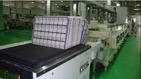
In printed circuit processing, ammonia etching is a relatively fine and complex chemical reaction process. On the other hand, it is an easy work. Once the process is adjusted, it can be produced continuously. The key is to keep the continuous working state once the machine is started, and it is not suitable to dry or stop. The etching process depends on the good working state of the equipment to a great extentFor example, no matter what kind of etching solution is used, high-pressure spraying must be used. In order to obtain neat line sides and high-quality etching effect, the structure and spraying mode of the nozzle must be strictly selected.
In order to obtain good side effects, many different theories have emerged, forming different design methods and equipment structures. These theories are often quite different. However, all theories related to etching recognize the most basic principle, that is, keep the metal surface in contact with fresh etching solution as soon as possible. The chemical mechanism analysis of the etching process has also confirmedIn ammonia etching, assuming that all other parameters remain unchanged, the etching rate is mainly determined by the ammonia (NH3) in the etching solution. Therefore, there are two main purposes for using fresh solution to interact with the etching surface: one is to flush out the newly generated copper ion; the other is to continuously provide the ammonia (NH3) required for the reaction.
In the traditional knowledge of the printed circuit industry, especially the suppliers of printed circuit raw materials, it is recognized that the lower the content of monovalent copper ion in ammonia etching solution, the faster the reaction speed, which has been confirmed by experience. In fact, many ammonia etching solution products contain special coordination groups of monovalent copper ion (some complex solvents), its function is to reduce monovalent copper ions (these are the technical secrets of their products with high reaction capacity). It can be seen that the influence of monovalent copper ions is not small. If the monovalent copper is reduced from 5000ppm to 50ppm, the etching rate will be more than doubled.
Because a large number of monovalent copper ions are generated during the etching reaction, and because monovalent copper ions are always tightly combined with the complex group of ammonia, it is very difficult to keep their content close to zero. Monovalent copper can be removed by converting monovalent copper into divalent copper through the action of oxygen in the atmosphere. The above purpose can be achieved by spraying.

 Dec. 20, 2019


