
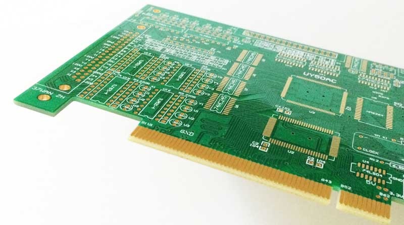
With the rapid development of PCB industry, PCB is gradually developing towards high-precision fine lines and small aperture. Generally, PCB manufacturers have the problem of electroplating film clamping. PCB film clamping will cause direct short circuit and affect the primary yield of PCB through AOI inspection. Serious film clamping or too many points can not be repaired, which will directly lead to scrapping.
Cause analysis of PCB film clamping
1. The current density of pattern plating is high and the copper plating is too thick.
2.There is no edge strip at both ends of the flying bar, and thick clamping film is plated in the high current area.
3.The set current of the fire cow fault is greater than that of the actual production board.
4.The C/S surface is hung upside down with the S/S surface.
5.The spacing is too small, and the plate with a spacing of 2.5-3.5mil is sandwiched with film.
6.The current distribution is uneven, and the anode of the copper plating cylinder is not cleaned for a long time.
7.Wrong current (wrong model or wrong area of input board)
8.The protection current of PCB board in copper cylinder is too long due to equipment failure.
9.Unreasonable layout design of the project, incorrect effective electroplating area of the drawings provided by the project, etc.
10.The line gap of PCB is too small, and the circuit graphics of highly difficult PCB are special and easy to clamp film.
Effective improvement methods on PCB film clamping
(1) Reduce the electric current density and appropriately extend the copper plating time.
(2) The plating copper thickness of the plate shall be appropriately thickened, the plating copper density of the drawing shall be appropriately reduced, and the plating copper thickness of the drawing shall be relatively reduced.
(3) The bottom copper thickness of the pressing plate is changed from 0.5OZ to 1/3OZ bottom copper pressing plate.Thicken the copper plating thickness of the plate by about 10㎛, reduce the electrical current density and reduce the copper thickness of the pattern plating.
(4) Purchase 1.8-2.0mil dry film for plates with spacing < 4mil for trial production.
(5) Other methods such as changing typesetting design, modifying compensation, shifting wire gap, hole cutting ring and PAD can also relatively reduce the generation of clamping film.

 Oct. 15, 2021


