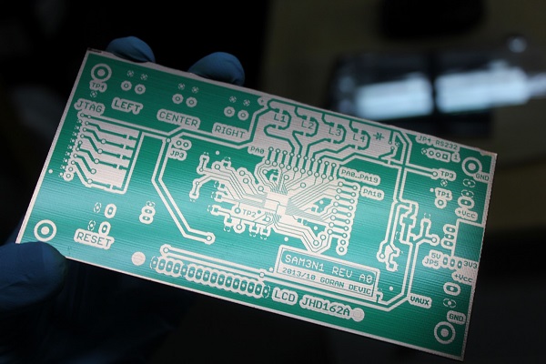
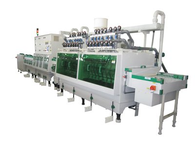
In the process of high-density image transfer, if the control fails, it is very easy to have quality problems such as infiltration plating, poor development or anti-corrosion dry film stripping.In order to further understand the cause of the fault, the causes and solutions of PCB unclean development are introduced below.
Infiltration plating
The so-called infiltration plating is that the plating solution is deepened due to the weak adhesion between the dry film and the surface of copper-clad foil, resulting in the thickening of the coating in the “negative phase” and the plated tin lead corrosion resistant layer, which brings problems to the etching. It is easy to scrap the printed circuit board, which is a key point to pay special attention to in production.The causes of infiltration during pattern electroplating are analyzed as follows:
1. Poor dry film development and overdue use
As mentioned above, the photoresist dry film is composed of three parts: polyester film, photoresist film and polyethylene protective film.Under UV irradiation, good adhesion between the dry film and the surface of copper foil is produced, which plays the role of anti electroplating and anti etching.When several films are used beyond the validity period, this layer of binder will fail, and the protective effect will be lost in the electroplating process after coating, resulting in infiltration plating.The solution is to carefully check the effective service cycle of dry film before use.
2. Effect of temperature and humidity on film sticking
Different dry films have their suitable film sticking temperature.If the coating temperature is too low, the adhesion between the dry film and the copper-clad laminate surface is poor due to the insufficient softening and proper flow of the resist film;If the temperature is too high, bubbles will be generated due to the rapid volatilization of solvent and other volatile substances in the resist, and the dry film becomes brittle and is not resistant to electroplating, resulting in warping and stripping, resulting in infiltration plating and scrapping.
If water-soluble dry film is used, the humidity in the air has a great influence on it.When the humidity is high, the adhesive of dry film can achieve good bonding effect when the coating temperature is low. Especially in the south, the temperature in summer is relatively high. A set of better temperature control parameters are explored from long-term practice. Under the condition of 20-250℃ and relative humidity above 75%, the film temperature is better below 730℃;When the relative humidity is 60-70%, the film temperature is 70-800℃;When the relative humidity is below 60%, the film temperature is higher than 800℃.Similarly, increasing the pressure and temperature of the film cot also achieved good results.
3. Long exposure time or insufficient exposure
Under UV irradiation, the photoinitiator absorbing light energy is decomposed into free radical initiator monomer for photopolymerization to form body molecules insoluble in dilute alkali solution. In order to make the best effect of each dry film polymerization, there must be an optimal exposure.From the definition formula of light energy, the total exposure e is the product of light intensity I and exposure time t. If the light intensity I is constant, the exposure time t is an important factor that directly affects the total exposure.When the exposure is insufficient, due to incomplete polymerization, the adhesive film swells and softens during the development process, resulting in unclear lines and even film falling off, resulting in poor combination between the film and copper;If the exposure is excessive, it will cause development difficulties, and will also produce warping and peeling in the electroplating process, forming infiltration plating.Therefore, the solution is to strictly control the exposure time, and each type of dry film should be measured according to the process requirements.
4. Poor development
After exposure, the copper-clad laminate pasted with dry film must also be developed by the PCB developer. Keep the unexposed dry film with the original composition, and the following reactions occur with the developing solution in the pcb developer: -COOH+Na+ → -COONa+H+
Among them – COONa is a hydrophilic gene, which is dissolved in water and peeled off from the dry film to expose the pattern to be electroplated on the whole board surface, and then electroplated .-COONa is the dry film component and Na + is the main component of the developing solution (Na2CO33% plus an appropriate amount of defoamer). If the developing is not accurate, there will be surplus glue in the graphic wire part, which will cause local copper plating failure and form waste and defective products, which is the most prone quality problem in the development section.
5. Exposure time is too long
When the exposure is excessive, the ultraviolet light passes through the transparent part of the photographic film and produces refraction and diffraction phenomena, and irradiates the dry film under the opaque part of the photographic film, so that the dry film which should not undergo photopolymerization reaction will undergo polymerization reaction after partial exposure, and the phenomenon of residual glue and too thin lines will occur during development.Therefore, proper control of exposure time is an important condition for controlling the developing effect.


 Dec. 18, 2019


